


-
Group News2023-05-17
- Dialogue with Top Bonding Technology Experts: How Wafer Bonding Transcends More than Moore | Jiazi Guangnian


The 'grafting' technology in the semiconductor industry.
Author | Zhao Jian
Moore's Law is the guiding principle for the development of the semiconductor industry. For half a century, the number of transistors that can be accommodated on integrated circuits has basically followed the trend of doubling every 18-24 months while reducing chip costs by half.
But today, as the chip manufacturing process enters 5nm or even 3nm, under the limitations of physical laws, Moore's Law has approached its limit, and it has become increasingly difficult to continue reducing the feature size of transistors in two-dimensional planes to improve chip performance.
Therefore, the development of new structures from two-dimensional planes to three-dimensional integration has become an important direction to surpass Moore's Law and promote the development of the semiconductor industry.
Wafer bonding "is a type of 3D integration technology.
Although not as popular as semiconductor concepts such as lithography machines and EDA, wafer bonding has a wide range of applications in fields such as MEMS (Micro Electro Mechanical Systems), CMOS (Image Sensors), DRAM (Dynamic Random Access Memory), and NAND (Computer Flash Memory).
Wafer bonding is a "grafting" technology in the semiconductor industry, which tightly combines two mirror polished chips through chemical and physical processes, thereby improving device performance and functionality, reducing system power consumption, size, and manufacturing costs.
Due to the enormous potential of wafer bonding in 3D integration, well-known companies such as Intel, Samsung, Huawei, Qualcomm, ROHM, TSMC, as well as numerous universities and research institutes, have conducted research on equipment, devices, and processes related to wafer level packaging bonding.
For example, Intel unveiled a new 3D hybrid bonding technology at the 2022 IEEE International Electronic Devices Conference, which increased power density and performance by 10 times.
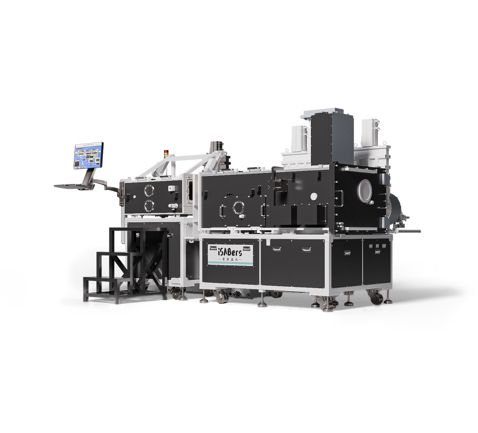
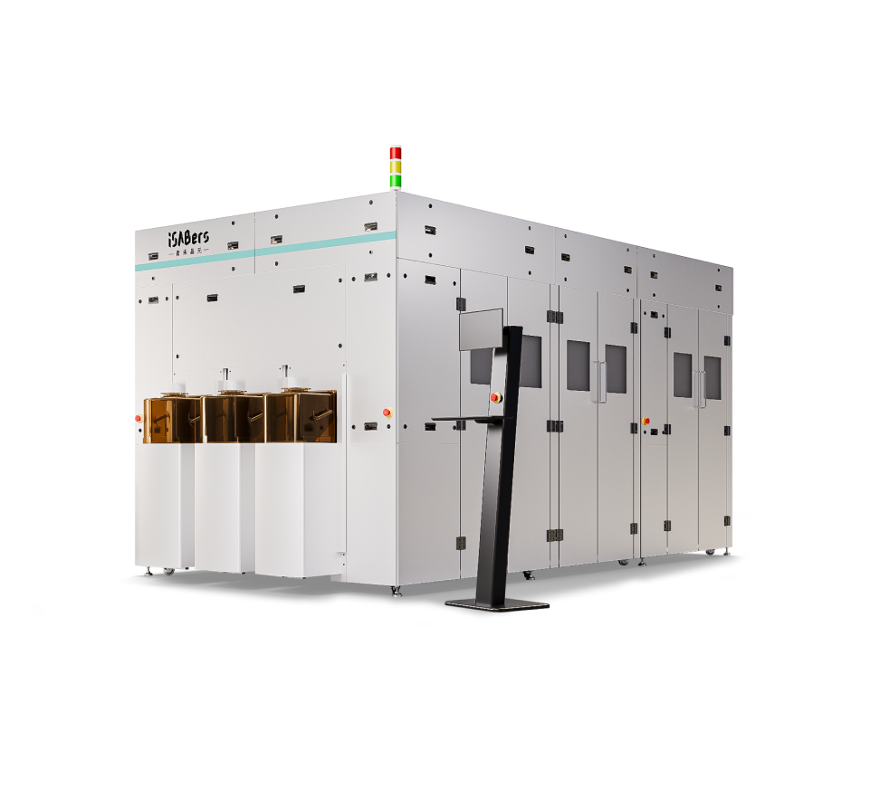
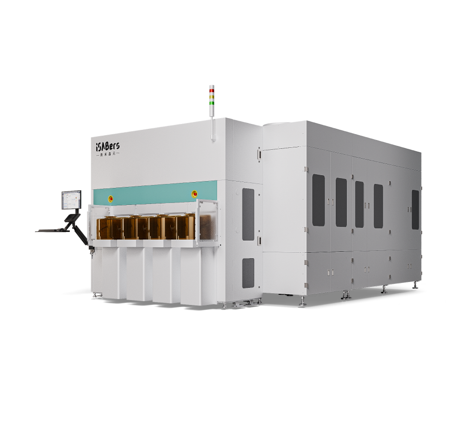
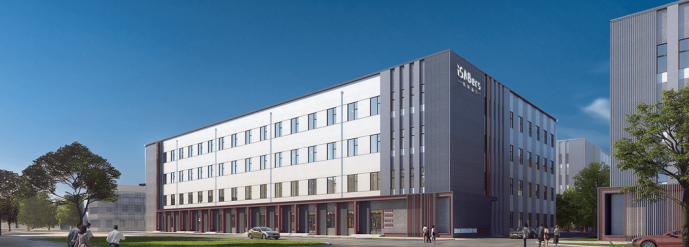
In China, wafer bonding is also an emerging direction for semiconductor entrepreneurship. Established in 2020, Zhongke Jinghe, which was previously invested by Huawei Hubble, is one of the representative companies.
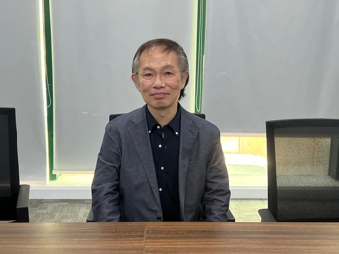
The parent company of Zhongke Jinghe, iSABers, has its chief scientist, Weichi Suga, who is an honorary professor at the University of Tokyo, former president of the Japan Electronic Packaging Society, and a leading figure in wafer bonding. Professor Suga began researching room temperature wafer bonding in the 1990s, which is currently the most advanced bonding technology direction.
Recently, "Kai Zi Guangnian" interviewed Professor Suga to explore the impact of wafer bonding on surpassing Moore's Law and promoting the development of the semiconductor industry.
1. Wafer bonding: one of the core technologies beyond Moore's Law

Jiazi Guangnian: For the semiconductor industry chain, the simplest classification is usually the three major links of chip design, chip manufacturing, and chip packaging and testing. Can you explain in layman's terms the position and role of "bonding" in the semiconductor industry chain?
Suga Weizhi: The semiconductor industry can be divided into "pre process" and "post process" from a technical perspective, and bonding technology is regarded as a technology of "post process" and "packaging". However, with the limits of semiconductor miniaturization and obstacles to integration in recent years, people have begun to recognize 3D integration as an important technology that surpasses previous technological barriers.
In the traditional semiconductor industry chain, design, manufacturing, and packaging testing are relatively independent, but now the situation has changed. Considering the integration of the entire system, bonding needs to be discussed in the pre process rather than limited to the post process, otherwise the entire system will not be able to complete it. This makes the entire process tight and seamless.
In the semiconductor industry, key cooperation plays an important role as the core technology of advanced packaging technology. In 3D integration, bonding technology is a key technology for stacking DRAM memory and NAND memory. In addition, the stacking of logic chips and memory also relies on the support of bonding technology. In addition, new devices in the fields of Si Photonics and photonics also rely on bonding technology for implementation.
Jiazi Guangnian: The physical and chemical principles of bonding technology were actually discovered and applied even before humans cut out the first wafer. But the true large-scale industrial application of wafer bonding only began after the 1990s. What is the reason?
Suga Weizhi: Since the practical application of SOI (Silicon on Insulator) wafer bonding, wafer bonding technology has truly begun to be applied. Prior to this, there was almost no use of wafer bonding technology in the industrial sector. Subsequently, with the emergence of industrial fields such as MEMS packaging, SAW filters, and Si Photonics, the number of fields that rely on bonding technology for implementation gradually increased.
Jiazi Guangnian: There are many classifications for wafer bonding, can you first help us sort out the types of bonding?
Suga Weizhi: The bonding method can be divided into two types: the bonding method of adding solder or other interconnecting intermediate layers between bonding materials, and the direct bonding method without intermediate layers.
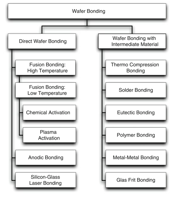
In Si and SiO2 wafer bonding, hydrophilic bonding is mainly used, which can bond in atmospheric environment and is widely used, but requires heating to 350 ° C; while surface activated bonding (SAB) requires vacuum environment but can bond at room temperature.
At present, research has begun on Modified SAB that combines these two methods. For direct bonding of metals, SAB is a room temperature bonding method, while traditional heating methods include thermal compression bonding (TC bonding) and diffusion bonding.
Jiazi Guangnian: Professor Suga has also been researching bonding technology since the 1990s, directly challenging the particularly cutting-edge room temperature bonding technology, which should have exceeded the understanding and imagination of many people at that time. What was your starting point and motivation at that time?
Suga Weizhi: Bonding itself is a simple method of utilizing the high surface energy properties of material surfaces. However, traditional techniques do not use this characteristic, but instead utilize the chemical reactions during the thermal activation process through heating. However, doing so will generate thermal stress and brittle reaction layers at the bonding interface, reducing strength and reliability. In order to fully utilize the characteristics of the surface, it is necessary to clean the surface to the extreme (surface activation), which requires environments such as ultra-high vacuum, but the cost of vacuum equipment is very high. At that time, the industry was not interested in it, and the academic community did not realize the necessity of matching it with research funding.
Why did I choose the more challenging room temperature bonding? This question is a bit difficult to answer. But personally, in various studies, I prefer this unconventional approach. I am more concerned with the problem itself, rather than just the way it is solved. I believe that only in this way can we achieve good results. I have always told my students not to follow the rules when thinking about problems. I have always believed that being faithful to principles is the shortcut when studying anything. In a sense, I may be a bit clumsy, but it could also be because I enjoy this approach, which is why I chose this challenge. But from the results, it may be good.
Jiazi Guangnian: What are the advantages and challenges of room temperature bonding?
Suga Weizhi: The advantage of room temperature bonding is that the bonding process can be completed at room temperature. Therefore, compared with the method of bonding by heating, room temperature bonding can achieve bonding of dissimilar materials without problems, avoiding bonding difficulties caused by thermal stress and reactions.
Whether it is traditional high-temperature wafer bonding or room temperature bonding, the challenge lies in the need for a very flat wafer surface (with a surface roughness of less than 1 nanometer), which is also one of the most expensive steps. There are currently various new attempts underway, not only in physical research, but also in the application of new technologies such as ion beams or plasmas.
Jiazi Guangnian: Is room temperature bonding a substitute for traditional high-temperature bonding? Or is it a parallel relationship?
Suga Weizhi: It is a parallel relationship. In the current situation, there is no need to deliberately shift to room temperature bonding technology to meet the needs that ordinary bonding technology can meet. But things that couldn't be done in the past may require the use of new technologies, and we can take new demands and application areas as development directions.
Jiazi Guangnian: What important advances have been made in bonding technology, especially ambient temperature bonding technology, over the past two decades? What are the important milestone events?
Suga Weizhi: Initially, we conducted surface activated room temperature bonding between metal metal and metal ceramic. In 1996, we first achieved silicon wafer bonding, and in 1997, we demonstrated hetero bonding of compound semiconductors. At the 2001 IEEE-ECTC academic conference, we first proposed the concept of "Bump interconnect" for Cu Cu direct bonding, which has become the foundation of current hybrid bonding technology and was rated as the best paper of IEEE-ECTC.
In 2010, we proposed an improved surface activated room temperature bonding method, which included an intermediate layer of nano adhesive layer for silicon, thus achieving room temperature bonding of glass and polymer films that was previously unattainable.
In addition, since 1998, we have collaborated with 11 semiconductor companies and industry academia alliances in Japan, and this collaboration with the industry continues to this day.
In the industry, Omron began mass producing MEMS sensors using Si surface activated bonding in 2012. Sony has been mass producing CMOS image sensors since 2016. It is highly likely that surface activated bonding technology will be widely applied in mixed bonding starting this year.
Jiazi Guangnian: Which international upstream companies have outstanding advantages in bonding technology?
Suga Weizhi: In the field of bonding equipment, Austria's EVG company holds a significant market share; But currently, there are only a few manufacturers in Japan in terms of surface activated bonding.
Jiazi Guangnian: What do you think are the development directions of bonding? What is your understanding of future bonding technology?
Suga Weizhi: The technology of room temperature bonding is basically mature. However, the equipment and parameter adjustment for practical applications are still far from complete. Due to the existence of various application scenarios, these issues will gradually be resolved in the future and become easier to use. At present, people are not very familiar with this concept, and some may find it unfamiliar. Now there are only one or two customized devices, and everyone is not quite sure how to use them. But I believe that with the promotion and popularization, these problems will gradually be solved.
2. Establishing a connection with Chinese semiconductors

Jiazi Guangnian: When did your cooperation with the Chinese semiconductor industry first begin? What was the opportunity at that time?
Suga Weizhi: In 2005, the University of Tokyo established its representative office in China (located in Wuxi), and we had various exchanges, but unfortunately, it did not promote effective industrialization.
Since 2012, I have been a visiting professor at the Institute of Microelectronics, Chinese Academy of Sciences, and have had many exchanges in my research field. But I think more time is needed to cooperate with China's semiconductor industry.
Jiazi Guangnian: What is the current development status of bonding technology in China? Which companies are doing well?
Suga Weizhi: As far as I know, advanced bonding technologies such as lasers are being developed in places like Tsinghua University. However, in terms of technology in the industrial sector, I have limited knowledge of China's unique technology. iSABers is one of the companies I am familiar with, and I also have expectations for its development.
Jiazi Guangnian: You are the Chief Scientist of iSABers. How did this collaboration begin? What is the opportunity?
Suga Weizhi: Over the past 35 years of bonding research at the University of Tokyo, more than a few Chinese international students (doctoral students) have made significant contributions. One of them is Mother Fengwen (General Manager of iSABers) of iSABers Company. He successfully utilized surface activated bonding technology to conduct bonding research on new materials such as SiC, GaN, and diamond. I think these jobs were one of the opportunities for the establishment of iSABers.
Jiazi Guangnian: What impressed you the most about iSABers company?
Suga Weizhi: Although iSABers has only been established for 3 years, they have quickly transformed their technology into products and incorporated many new ideas, so we can expect them to achieve tremendous development.
Jiazi Guangnian: Japan is at the forefront of the world in areas such as semiconductor materials and equipment. Can you compare the development of the semiconductor industry in China and Japan from a personal perspective and provide suggestions for the Chinese semiconductor industry.
Suga Weizhi: Japan is at the forefront of the world in areas such as semiconductor materials and equipment. However, semiconductor technology is not just about purchasing equipment and arranging them together. I believe that through self challenge, new wisdom, technology, and industries can be nurtured. The power of capital is certainly important, but cultivating talents and independently developing technology are more important than anything else.
This may be more like a warning bell for the gradual decline of the Japanese industry, rather than just a suggestion for China's semiconductor industry.
-
Latest News
- 2025-05-01
- Pay tribute to the strivers in the semiconductor industry and wish you a happy May Day!
-
Latest News
- 2025-04-21
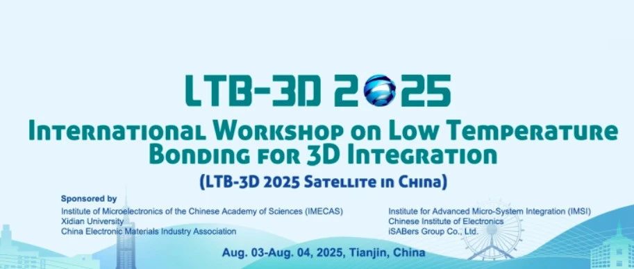
- iSABers Co-hosted – 2025 China International Seminar on Low-Temperature Bonding and 3D Integration Technology Invites You to Participate
-
Latest News
- 2025-03-28
- iSABers SEMICON Moment: Offline Innovation Sharing Session Successfully Held
-
Latest News
- 2025-03-27
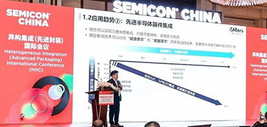
- iSABers' SEMICON Moment: Showcasing China's Solutions for Advanced Bonding Technology
-
Latest News
- 2025-03-21
- SEMICON In-Person Advanced Bonding Technology Breakthroughs Symposium